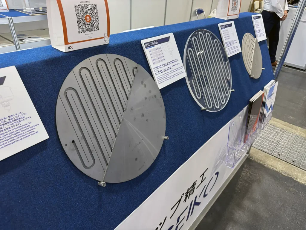
Components that operate in extreme environments—such as semiconductor manufacturing equipment—require the “complete elimination of metal contamination” and “complex internal cooling and flow path structures.” However, achieving this with hard and brittle ceramics has long been considered difficult.In this article, we examine the approach that enables complex three-dimensional structures—and its business implications—through the “diffusion bonding” technology presented by Top Seiko Co., Ltd.
1. [Core Technology] No adhesives or screws required. “Diffusion bonding” that integrates materials while they remain in a solid state.
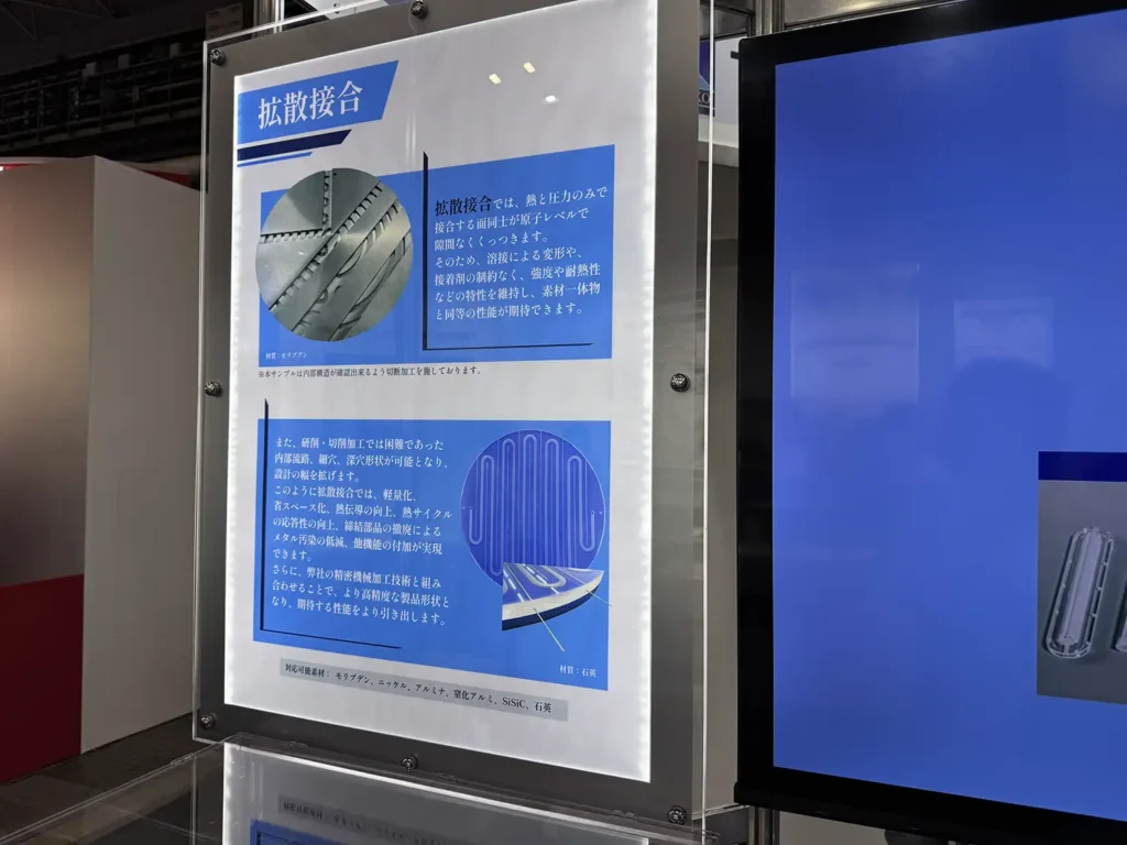
“Diffusion bonding,” a technique employed by Top Seiko, involves bringing the materials to be joined into close contact while they are still in a solid state, and then using heat and pressure to move the atoms at the interface and form a bond.
Its most distinctive feature is that it uses absolutely no “foreign materials,” such as adhesives or solder. As a result, the physical and mechanical properties of the materials remain unchanged before and after joining, and their heat resistance is not compromised.By using this technology to bond plates that have been precision-machined in advance to include microscopic grooves and holes, it becomes possible to form “complex three-dimensional internal flow channels”—which previously could not be machined from a single solid block—while preserving the pure properties of the ceramic material.
2. [Key Points] A “Mono-Think” Perspective
What is particularly noteworthy is the “overwhelming purity” of this technology’s system architecture.
The beauty of creating complex modules using only pure materials—without relying on external elements such as fastening bolts or adhesives—is an extremely logical approach for next-generation manufacturing processes that tolerate absolutely no impurities.In particular, diffusion bonding between ceramics—which are highly prone to thermal expansion and cracking—is an extremely delicate and challenging technique that requires precise control of temperature and pressure. It can
truly be described as a level of craftsmanship worthy of the “Japan Brand” label.
This integration of advanced precision machining and bonding technologies—which cannot be easily replicated—is dramatically expanding the scope of design freedom.
3. [Impact from a Management Perspective] Improved Yield and Adaptability to Next-Generation Equipment
The adoption of this technology directly contributes to quality control and performance improvement in cutting-edge industries.
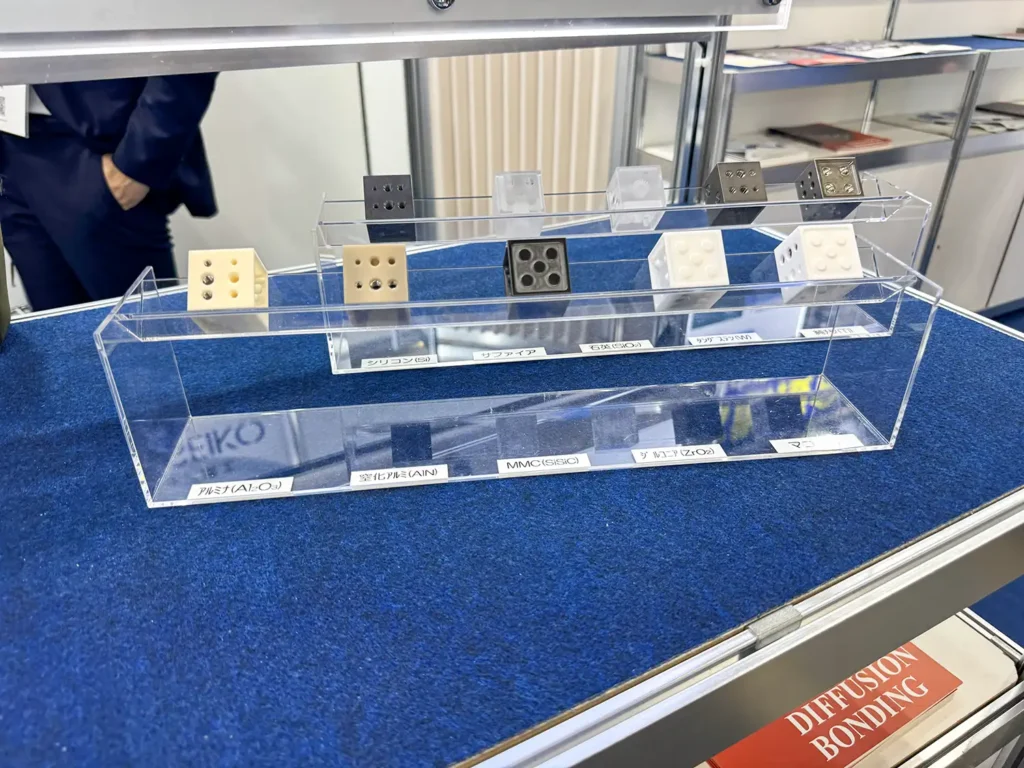
For example, if shower heads and vacuum chucks used in semiconductor manufacturing facilities were constructed from pure ceramics (such as alumina or aluminum nitride) using this diffusion bonding technique, concerns about metal contamination would be eliminated at the root.Furthermore, if gas injection and cooling efficiency are optimized through uniform internal flow paths, product yield will improve dramatically. Component designs that break through these limits will directly lead to a dramatic leap in the performance of end-users’ equipment. In the field of cutting-edge technology, which continues to advance, this “technology that makes the impossible possible” is sure to become an extremely powerful strategic asset for securing dominance in the next generation.
[Reporting, Writing, and Photography]
The mono-think Editors
A web media outlet that explores the cutting edge of Japan’s “manufacturing” and “infrastructure” from the perspective of active IT engineers, offering a unique perspective.
[Research Cooperation & Related Links]
TOP SEIKO
Adhesives & Joining EXPO